Pages

Tuesday, February 28, 2012

TI introduces 1st quad ARM A15 core basestation on a chip for LTE/LTE-A at Mobile World Congress

TI's TCI6636 integrates 4 ARM A15 cores with 8 C66x DSPs, for a complete LTE/LTE-Advanced base station on a chip

Texas Instruments (TI) has introduced the next generation of their multicore system on a chip (SOC) architecture,  Keystone II, at the Mobile World Congress this week. The company also announced the first device that employs the new architecture, the TCI6636 base station on a chip. Tom Flanagan, Director of Technical Strategy for Wireless Base Station Infrastructure at TI, says that in the Keystone II, TI has upgraded the underlying silicon technology from 40nm to 28nm.  The company had developed twelve 40nm Keystone chips in just 18 months, he said, each with ~1B transistors. With the new process node, TI has increased transistor density to be able to integrate 2-3B transistors.

TI designed the TCI6636 to be used in the high-end of the small cell market segment, or to be grouped together to make a macro cell while lowering cost and power requirements. In the TCI6636, TI has integrated ARM's latest A15 cores, but with their own proprietary cache coherency system. TI's Keystone II memory system increases support from 8 cores in the previous Keystone architecture, to up to 32 cores in the new architecture. Flanagan says that TI's strategy is to use standard cores from ARM, and to implement their own enhancements around the cores, in order to retain the full benefits of the ARM ecosystem. The TI designs can still achieve up to 4X performance improvement over competitors,according to Flanagan.

In the TCI6636, TI adds accelerators to the base Keystone architecture for wireless infrastructure applications, with integrated switch functions in the I/O blocks.  The new SOC has eight C66x DSP cores, each with a dedicated 1MB memory subsystem. The general purpose processing is performed by a quad-core configuration of 4 ARM A15s, sharing 4MB of memory. An additional 6MB of memory is shared across the 12 DSP + CPU cores, for a total of 18MB of on-chip memory. Along with large on-chip memory, TI has added dual, 72b DDR3 interfaces for external memory. Flanagan says that this "beast" of a fast memory sub-system accounts for much of the performance increase in the TI6636.

In regards to the processor performance, Flanagan says that the 4 ARM A15s cumulatively provide 17.5 Dhrystone MIPS (Million Instructions Per Second), while the 8 DSP cores achieve 320 billion multiply accumulates per second (GMACS), and 160 billion floating-point operations per second (GFLOPS). Flanagan said that TI worked closely with ARM on development of the A15 core, and the TI6636 is the first implementation of a quad configuration, and the first where the cores are operated at higher than a 1GHz clock rate.

With the introduction of the TI6636, TI now has a range of three base station on a chip SOCs, from the 40nm ARM8-based TMS320TCI6612 and TMS320TCI6614 that the company introduced at the Femtocell World Summit in London last year, to the new 28nm ARM A15-based TCI6636:
  • TCI6612 supports Cat 1–5 LTE (max. of 300Mbps downlink, 75Mbps uplink) and HSPA+, and can be operated in dual (4G/3G) with up to 64 users.
  • TCI6614 adds advanced receiver algorithms, and more sophisticated schedulers, for simultaneous dual-mode support of up to 128 users.
  • TCI6636 adds to the 6614 capability with Cat-7 LTE support (300Mbps downlink, 150Mbps uplink), and  LTE-Advanced support for a 40 MHz bandwidth with carrier aggregation, and up to 256 users.
Three TCI6636 SOCs can be grouped together to form a macro cell base station

Flanagan outlined how features built in to the TCI6636 can lower the cost and power of a conventional macro cell architecture.  By connecting three of the devices with TI's hyperlink bus, the network processor for system control and packet processing can be eliminated at a savings of ~30 watts, saving $50 of cost. He estimates that elimination of a separate ethernet switch saves 10 watts and $200, while the built-in Serial Rapid IO (SRIO ) switch saves 10 watts and $125. The multi-antenna interface in the TCI6636, which is typically implemented in an FPGA, can save 25 watts of power and provides a cost saving of $250, according to Flanagan's calculations. The bottom line, he says, is a cumulative savings of 75 watts and a cost reduction of $625. Further power savings are possible, by shutting down one of the SOCs in base stations where full capacity is not required in off-peak hours.

TI expects to begin sampling the TCI6636 SoC in the second half of 2012.

Related articles

Freescale claims highest performance macrocell basestation on a chip at Mobile World Congress

Freescale's B4860 provides a complete basestation on a chip for LTE and LTE-Advanced macrocells

With their announcement of the B4860 at Mobile World Congress, Freescale Semiconductor is extending their line of QorIQ Qonverge basestation on a chip SOCs from picocells up through to large macro cells. In August of last year, Freescale began sampling their 45nm PSC9132/ 31/ 30 for femto and pico cells. The B4860, which Freescale will manufacture in a 28nm CMOS process, supports three 20MHz sectors of LTE, for metropolitan applications with hundreds or thousands of users.

Stephen Turnbull, Multicore & Host Processor Portfolio Manager at Freescale, says that the B4860 can achieve a download (DL) rate for LTE of 300Mbps, and an upload rate of 150Mbps. Turnbull also says that the macro basestation SOC is fully compliant with the 3rd Generation Partnership Project's (3GPP) Release 10 specification for LTE-Advanced, supporting 60MHz sectors at 1.2Gbps DL and 600Mbps UL, for a total data throughput of 1.8Gbps on Frequency Domain Duplexing FDD-LTE paired spectrum. The B4860 also supports WCDMA, TD-SCDMA, and GSM.

Freescale designed the B4860 for flexibility to support conventional Base-Band Units (BBU) at a macro cell site, for pooling of resources in a Cloud-based RAN (CRAN) connected to Remote Radio Heads (RRH) over Common Public Radio Interface (CPRI), or for use in heterogeneous networks with a mix of small and large cells.


Like other devices in the QorIQ family, such as the T4240 and T4160 for wireless backhaul applications, the B4860 architecture employs quad clusters of the dual-thread, 64-bit e6500 Power Architecture cores, along with the 128b AltiVec Single-Instruction Multiple-Data (SIMD) vector processor. This is the same architecture which Freescale simulations show to have achieved the highest CoreMark benchmark performance score ever recorded for an embedded processor.


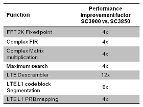
For baseband processing, the B4860 adopts a heterogeneous multi-core architecture, with three sets of dual StarCore SC3900 DSP cores, each pair sharing 2MB of L2 cache. Freescale benchmarks show the SC3900 DSP to provide 4X the performance of the previous generation SC3850, such as the cores in the PSC9132 basestation SOC for picocells. Freescale has announced that the SC3900 recently achieved the highest fixed-point BDTIsimMark2000™ benchmark score ever recorded by analysis firm Berkeley Design Technology, Inc. (BDTI). At 1.2 GHz, the SC3900 core registered a performance benchmark score of 37,460, which Freescale says is 2X higher than competitive DSPs on the market.

The Maple-B3 cores offload the DSPs to provide Layer-1 acceleration, and actually occupy a larger portion of the silicon real estate than the other cores, according to Turnbull. He says that the high level of integration provides the equivalent functionality of five components; 3 DSPs for Layer-1 processing, and a Serial RapidIO (SRIO) switch, connecting to a separate multicore processor for Layer-2 and Layer-3 transport and control processing. Freescale expects to begin sampling of QorIQ Qonverge B4860 devices in Q2 2012.

Related Articles

Monday, February 27, 2012

Synopsys speeds up protocol verification for SOC communication interfaces

The new Synopsys VIPER architecture is a protocol-centric system
for verification of communication interfaces on SOCs

Synopsys Inc. has announced a new set of tools in their family of Discovery Verification Intellectual Property (VIP) products, focused on analysis and debug of communication protocols such as Universal Serial Bus (USB), Double Data Rate (DDR) memory interfaces, and Peripheral Component Interconnect Express (PCIe).

Neill Mullinger, Group Marketing Manager for VIP at Synopsys, says that the company has written the new library entirely in SystemVerilog, based on an architecture they have dubbed "VIPER", with native support for the industry-standards: Universal Verification Methodology (UVM), Verification Methodology Manual (VMM) and Open Verification Methodology (OVM). Mullinger says that by writing the new VIP family completely in System Verilog, the same language which verification engineers are typically using for their testbenches, the inefficiencies and overhead associated with plugging in legacy VIP written in 'e', VERA, or C-language models can be eliminated.

By incorporating a higher-level class library, Synopsys has architected the VIP so that users can compile just what they need for their chosen methodology, without carrying the overhead of extraneous components, says Mullinger.  To make the VIP easier to use, Synopsys provides built-in test plans with "Quick Start" instructions in Hyper Text Markup Language (HTML) form, which guide verification engineers on how to configure the VIP for their tests.

Synopsys Protocol Analyzer highlights bottlenecks or errors in a communication interface

To make the VIP easier to debug, Synopsys has also developed a Protocol Analyzer, a Java-based tool that the company designed with an awareness of the verification requirements for various communication protocols. Hooks are built into the VIP so that users can easily monitor signals with the Protocol Analyzer. Users can monitor activity in a communication interface on a transaction by transaction basis, highlighting the relationships of data transfers, packets, and handshaking across the protocol hierarchy. Tests of multiple protocols can be graphically linked to synchronize display of data communication across an interface. Since the data for the Protocol Analyzer is generated directly by the VIP, Mullinger says that all major simulators are supported.


Synopsys has enhanced their portfolio of VIP through their recent acquisitions of nSys Design Systems, and ExpertIO, and includes USB 3.0, ARM AMBA AXI3, AXI4, ACE, HDMI, MIPI (CSI-2, DSI, HSI, etc.), Ethernet 40G/100G, PCI Express, SATA, OCP. For a  complete list see http://www.synopsys.com/VIP/.  The video embedded below provides Synopsys' introduction to the new Discovery VIP, from several of the company's R&D and marketing staff, and a customer testimonial from Cavium.

Mobile World Congress: Broadcom enables lower priced Android ICS smartphones with new family of processors

At the opening of the Mobile World Congress in Barcelona today, Broadcom announced development of a family of smartphone platforms, which the company has designed to enable handset manufacturers to produce mid- to low-tier handsets optimized for the Android Ice Cream Sandwich operating system. The platforms will include a range of new single/dual-core application processor Systems on a Chips (SoCs) integrated with HSPA/ HSPA+ modems, along with a family of ICs that provide Bluetooth, WiFi, GPS, and Near-Field Communications (NFC) connectivity.

In a preview of the announcement, Bob Rango, EVP and GM of Broadcom’s Mobile and  Wireless Group, emphasized the need to utilize unlicensed spectrum to offload smartphones from cellular networks, in order to reduce the strain of increasing video consumption in mobile devices. On February 15, Broadcom had announced the BCM4334, which supports dual-band 2.4GHz and 5GHz 802.11n WiFi concurrent with Bluetooth (BT) 4.0, including capabilities for Wi-Fi Direct and Wi-Fi Display. Rango said that through a combination of the 40nm LP process and extensive use of sleep power modes, the company has been able to reduce power consumption for the combination WiFi/BT by 30-50% from the previous generation device. He expects that the phones with the BCM4334 will appear in the 2nd quarter of this year.

In the February-15 announcement, Broadcom also announced the BCM43241 for tablets and "superphones", which supports 2x2 Multiple Input Multiple Output with 20MHz or 40MHz 802.11n WiFi channels, along with Bluetooth 4.0 and an FM radio on a single SoC.

The first 40nm LP smartphone processor in Broadcom's set of MWC announcements, for lower-tier handsets, is the BCM21654G. The BCM21654G integrates a single 1-GHz ARM Cortex A9 processor, with a 7.2/5.8 Mbps HSPA modem, and low-power VGA video support with a 7GFLOP Graphics Processor (GPU). Rango said that this new chip will replace the previous generation SoC, which powers the Samsung Galaxy Y Series of Android Gingerbread phones that are currently popular in India and Asian market, and also powers Samsung Bada OS phones. The BCM21654G will enable these low-end phones, which typically sell for US$150 unsubsidized, to now run the most advanced version of the Android operating system.

Moving up in performance, the BCM28145 integrates dual ARM Cortex A9 cores running at up to 1.3GHz clock rates, in an architecture that increases graphics performance to 24GFLOPS, with Broadcom's VideoCore multimedia engine. The BCM28145 provides an integrated HSPA+ release-8, category-14 modem supports 21Mbps download, 5.8Mbps upload and Class 33 EDGE support. Rango said that the BCM28145, which will be manufactured in phones set to appear later this year, is equivalent to the two-chip combination of the Texas Instruments OMAP-4 processor and Infineon baseband chip, in Google's current flagship Galaxy Nexus phone.

The top of Broadcom's new line of processors is the BCM28155, which takes the BCM28145 and improves video performance from 720p to 1080p at 60 frames per second (fps). A key  to the performance, says Rango, is the VideoCore processor, a capability which the company acquired through their purchase of Alphamosaic Limited in 2004. Rango foresees the BCM28155 lowering the price point of smartphones that currently cost $500-$600 unsubsidized, running Android Ice Cream Sandwich, to the $250 to $300 level within the next year. Broadcom has added the capability for Android to support dual Subscriber Identity Module (SIM) cards, which is a common requirement in emerging markets.

Sunday, February 26, 2012

Marvell Introduces Big/Little 3-Core Apps Processor in TDD- LTE Platform at Mobile World Congress

Marvell is introducing three smartphone platforms at MWC, with the new PXA2128 multi-core application processor.

Marvell Technology Group is introducing three new smartphone reference designs at Mobile World Congress this week, with an emphasis on support for TDD-LTE (Time Division Duplexing) and TD-SCDMA (Time Division Synchronous Code Division Multiple Access) networks, such as those being developed by China Mobile. Clearwire, in the U.S., is in a joint development with China Mobile for TD-LTE development. 

Specifications for Marvell's PXA1202 TD-SCDMA modem
To construct the reference designs Marvell is introducing a new multi-core applications processor, the PXA2128, which they have paired with their multi-mode modem chips: the PXA1202, PXA1802 and PXA1801. Marvell introduced the PXA1202 at PT/EXPO Comm last year, shortly after the announcement of the PXA1801 "World Modem". The PXA1801 supports FDD-LTE (Frequency Division Duplexing Long Term Evolution) and TDD-LTE, along with DC-HSPA+ (Dual Carrier Evolved High-Speed Packet Access) for WB-CDMA (Wideband Code Division Multiple Access) and TD-SCDMA, and EDGE (Enhanced Data rates for GSM Evolution).

Specifications for Marvell's PXA1802 modem, which the company designed
with an emphasis on on TD operation, for TDD-LTE and TD-SCDMA.
Dr. Lu Chang, Director of Mobile Products at Marvell,  says that the PXA1202 is the world's first to support DLDC (Downlink Dual Carrier) for TD-HSPA+, enabling 3X faster download on existing TD-SCDMA networks. The PXA1802 supports both Category 4 TDD-LTE and FDD-LTE, with a maximum download (DL) rate of 150Mbps, and an upload (UL) rate of 50Mbps. The difference between the 1802 and 1801, says Chang, is that the emphasis in the 1802 is on TD modes, supporting handoff from TDD-LTE to TD-SCDMA. Marvell sees the PXA1802 being used in high-end smartphones, paired with an application processor, or in MiFi portable hotpot devices, paired with a separate WiFi radio chip. The PXA1202 is a scaled down version, or subset of the 1802 says Chang, for low-cost 3G MiFi and smartphone applications.

The Marvell PXA2128 marks a trend toward a big/little mix of processor cores in mobile application processors, such as NVIDIA's 4-plus-1 architecture in the Tegra 3. Marvell employs a hybrid symmetrical multiprocessing architecture, said Chang, with dual ARMv7 cores that are comparable to the Cortex A9, combined with a third, smaller core for low power operation. Marvell was able to optimize the ARM cores for performance-power tradeoffs, since they hold an ARM architectural license. Chang says that the processor is capable of supporting all releases of Android, including Ice Cream Sandwich. Marvell is currently sampling the PXA2128 to its lead customers.

Intel boosts Medfield smartphone platform with unveiling of developer toolkit at Mobile World Congress

The Intel GPA Frame Analyzer includes a task time visualization panel (top),
a scene overview panel (middle), a render target viewer (right), and a
tabs panel that enables developers to change state for what-if analysis.


At the 2012 International Consumer Electronics Show in January,  Intel announced that their first smartphone incorporating the Atom Medfield processor, the K800, would be released in China by Lenovo. The company also announced that they would release a smartphone reference platform for developers. At the Mobile World Congress (MWC) this week in Barcelona, Intel is demonstrating a suite of visual computing tools for their new smartphone platform, with the unveiling of a port of the company's Graphics Performance Analyzers (GPA). 

Intel says that their developer tools will support the Lenovo K800 as well as future Intel-powered Motorola devices. The company describes GPA as "an easy-to-use suite of optimization tools for analyzing and optimizing games, media, and other graphics intensive applications." Game application developers will be able to use the tools to conduct performance and power analysis. Intel says that the GPA suite of tools have been used by PC game and media application developers for years, to help analyze and optimize PC game performance. Now, Intel has adapted the suite of tools for the use of mobile developers, with the objective of faster game apps for users of Intel smartphones.

At MWC, Intel's demo includes connecting an Intel smart phone to an Ultrabook PC, via a USB connection. A 3D gaming scene from the GLBenchmark serves as the workload on the phone for the test. Developers can analyze real time charts of CPU load and power dissipation while the game scene is running, which are generated by Intel's GPA System Analyzer running on the PC.


Intel is also showing how game application developers can exercise and run “what if experiments” on different parts of the smart phone platform for performance tuning. At this point Intel considers the features that they are demonstrating in GPA to be an early engineering demonstration, to show proof-of-concept. Intel says that they have not yet implemented all of the current metrics that are available in GPA, in the smartphone development suite. The company cautions that the demo is not intended for developers to draw conclusions regarding actual platform or game performance. Your results may vary.

The video that is embedded below provides an introduction to GPA. Developers in the U.S. can look for more announcements regarding the Intel smartphone at the Game Developers Conference in San Francisco, March 5-9. The company will be providing more details at GDC, following on the preview demo which they will show to a group of developers at MWC.


Saturday, February 25, 2012

EDITORIAL: Mobile OS Wars vs. The Cloud. Are Google, Apple, Microsoft, RIM, et al wasting their time?

In a recent interview on the Gerson Lehrman Group (GLG) Research professional community website, G+ (not to be confused with Google+, which comes up on top of the list if you search for G+ on Google),  Charlie Kindel - former GM for the Windows Phone developer experience at Microsoft, criticized companies such as Google, Apple and his former employer for "wasting time building mobile operating systems". "They are all fundamentally the same", he said.

Kindel did say that he expects development of new mobile OS platforms to "plateau", but that fragmentation would actually increase.  He particularly focused on Google's Android operating system, saying that he was "personally disappointed that Google is doing so well, because it is a detriment to having a really easy-to-use user experience."  In apparent contradiction to his statement that all mobile operating sysems are essentially the same, Kindel said that he would not recommend an Android phone to a non-technical person. He did not say if he would recommend a Windows Phone as an alternative. 

Perhaps the U.S. population is getting more technical then. The latest (December 2011) mobile platform market share study from comScore shows that Android actually increased both its #1 market share, and lead over iOS, from 44.8% vs. 27.4% in September-2011, to  47.3% vs.  29.6% in December.


In Kindel's opinion, the mobile industry "should be focusing on creating end user value through the creation of powerful cloud services", because consumers don't want to be tied to a particular device. Creating a more seamless experience across platforms, from the smartphone to personal computer (whatever form it takes), to the living room entertainment system, is an area that Google, Apple, and Microsoft are each working on. Google is taking Android into the television as well as other connected devices, through Android @Home, and manufacturers are also installing Android interfaces in automobiles and all forms of consumer electronics. Apple has Airplay, and Apple-TV, but their closed operating system limits the number of ways they can connect with consumers. Though, with US$100B in the bank, they could easily pursue new markets if they chose to.

The question then is this:
Now that the mobile platform war is a 2-horse race, who do you think is better equipped to deliver the seamless cloud-based experiences... Apple or Google?
We posed this question to the G+ community, and the responses so far highlight some of the issues. Apple's closed system is both an advantage and a disadvantage. Google needs to deal with security-related concerns. Will Amazon leverage their success with the Kindle Fire, and its customized version of Android, into more cloud-based consumer experiences?

The cloud is looking a lot like the weather. Everybody talks about it, but what are they doing about it? 

We would like to hear what you think. Leave a comment here, or in the G+ community if you are a member, or send us an email here at the EE Daily News to share your thoughts.

Friday, February 24, 2012

Texas Instruments to perform LTE demo of 1.5GHz CMOS DAC for 3G/4G basestations at Mobile World Congress

At MWC, TI will demo their LTE TSW30SH84EVM transmitter solution, with the new 1.5GHz DAC34SH84
At the Mobile World Congress (MWC) in Barcelona next week, Texas Instruments (TI) will demonstrate a new 16bit/1.5Gsample/second (GSPS), 4-channel Digital-to-Analog Converter (DAC), the DAC34SH84. Chuck Sanna, Marketing Manager for High Speed Products at TI, says that the DAC34SH84 is 50% faster, and uses 50% less power than any other 16-bit DAC alternative, dissipating 362 mW/channel at 1.5 GSPS. TI is targeting the DAC at applications in 3G, LTE, GSM and WiMAX wireless base stations and repeaters, microwave point-to-point radio, Software Defined Radio (SDR), and waveform generation systems.

Sanna says that by packaging the DAC34SH84 in a Ball-Grid Array (BGA) package, TI was able to provide a 32b-wide input data bus, that supports data rates up to 750 MSPS.This provides supports 600-MHz of complex RF bandwidth, according to Sanna. The company is manufacturing the DAC in one of TI's internal CMOS processes, but Sanna could not provide details on the process node

  • Multi-DAC synchronization
  • Selectable 2×, 4×, 8×, 16× interpolation filter
    • Stop-band attenuation >90 dBc
  • Flexible, on-chip mixing 
    • Two independent fine mixers with 32-bit Numerically-Controlled Oscillators (NCO)
    • Power-Saving Coarse Mixers: ±n × fS/8
  • High-Performance, Low-Jitter Clock-Multiplying PLL
  • Digital I and Q Correction - Gain, Phase and Offset
  • Digital Inverse Sinc Filters
  • 32-Bit DDR Flexible LVDS Input Data Bus
    • 8-Sample Input FIFO
    • Supports Data Rates up to 750 MSPS signals
    • Data Pattern Checker
    • Parity Check
  • Temperature Sensor
  • Differential Scalable Output: 10 mA to 30 mA
  • 196-Ball, 12-mm × 12-mm BGA
Evaluation Boards
TI is releasing the DAC34SH84 along with the TSW30SH84EVM a complete RF signal chain evaluation module. The evaluation module adds TI's  TRF3705 IQ modulator and LMK04800 ultra-low jitter clock cleaner with Dual Loop Phase Locked Loops (PLLs) to form a complete transmitter evaluation card.TI will be demonstrating operation of the TSW30SH84EV, for generating 20MHz channel bandwidth LTE signals, at MWC next week.  

To enable high-bandwidth pattern generation for testing the DAC34SH84, or for use as a high-speed Analog-to-Digital Converter capture card, TI is also releasing the TSW1400EVM. The TSW1400EVM enables testing of 16-bit ADCs and DACs, and includes 1GB of memory, that enables 512Msample depth of data capture. 

For simple pattern capture, TI is releasing the TSW1405EVM evaluation card, which comes without memory but supports a 64k sample depth with the ability to collect data on up to eight channels concurrently. The TSW1405EVM integrates a Lattice Semiconductor ECP3 FPGA on-board, to enable interfacing to many of TI’s Low-Voltage Differential Signaling (LVDS) output ADCs.

As a complement to the TSW1405EV, for pattern generation testing of DACs, TI is releasing the  TSW1406EVM evaluation card. The TSW1406EVM also works with a software package that TI provides with a Graphical User Interface (GUI), which is compatible with the entire TSW1400 family. A demo is included with the software for generating a 20MHz LTE carrier.As part of their MWC demo, TI will run the DAC in a loop-back to the ADC12D1800RF RF sampling ADC, which TI picked up with their acquisition of National Semiconductor. Each of the EVM evaluation cards contain USB interfaces for testing with a PC.

Price and Availability

The TSW30SH84EVM is available now for a suggested retail price of US$499. TI is currently providing sample quantities of the DAC34SH84, and is planning to have production quantities Q2 of 2012, with a suggested retail price of US$78 for 1,000 units.


The TSW1400EVM is also available now, for a suggested retail price of US$649. The TSW1405EVM and TSW1406EVM will be available in March 2012, for a suggested retail price of US$99.


Thursday, February 23, 2012

Samsung at ISSCC: Quad-core Exynos apps processor relies on skillful analog IC design.

Samsung's new 32nm Exynos Application processor will be
produced in both dual-core and quad-core configurations.
At the International Solid State Circuits Conference this week, Samsung provided details of their next-generation Exynos mobile applications processor in their paper on "A 32nm High-k Metal Gate Application Processor with GHz Multi-Core CPU". Dr. Se-Hyun Yang, Principal Engineer for SoC Development at Samsung, delivered the presentation on Exynos, and conducted a demonstration of the device in a smartphone reference platform during the Industrial Demonstration Session (IDS) on Tuesday evening.

Exynos is either a Dual or Quad ARM-v7A Cortex A9-based architecture, which Yang says is capable of operating up with a CPU clock at up to 1.5GHz, and down to as low as 200MHz. Each CPU core includes a full hardware vector floating-point unit and a 64-bit ARM 64-bit NEON Single-Instruction Multiple Data (SIMD) multimedia engine. The cores share a 1MB L2 cache, with a Snoop Control Unit (SCU) to manage communications between the cores and the memory subsystem. The Graphics Processor Unit (GPU) uses quad pixel processors plus a geometry processor and 128KB of dedicated L2 cache, and supports OpenGL ES 1.1/2.0. The DRAM controller provides a 6.4GB/s (i.e. 16b @400MHz) dual-port interleaved DRAM interface for LPDDR2, DDR2 and DDR3 memories.

Managing Power
Yang said that the migration to Samsung's 32nm High-K Metal Gate (HKMG) process, with 1/100th the gate leakage of the predecessor 45nm poly-Silicon gate process, was the first key to managing power on the new applications processor. Process engineers can target either performance or low power in the HKMG process. With the same leakage as the 45nm process, a 32nm HKMG design would yield a 40% improvement in delay, said Yang. Alternatively, by targeting the same timing performance, leakage would be reduced by a factor of 10.

In Exynos, each voltage domain has independent voltage and frequency options, with additional power-gated sub-domains to enable blocks to be completely shut off. The processor employs a total of four major power domains: for the CPU cores and L2 cache, GPU, memory interface, and audio/video IP blocks. The CPU cores have their own power sub-domains, and the L2 cache is split into two sub-domains with retention registers. Each core can be turned on and off independently, or put into a state with half of the cache turned off. Each of the audio/video media IP blocks can also be turned off independently.

Designers control the power of the L1 cache by placing power-gating switches around the periphery at design time, so they can minimize voltage drop on the rails. Samsung integrates power switches directly into the L2 cache, in order to minimize die area.

Yang stated that games are the most challenging applications for power management in mobile processors. In a dual-core example, he showed how the processor activity ramped up from a 20% load to 95%. Samsung utilizes both Dynamic Voltage and Frequency Scaling (DVFS), and power gating, to manage the workload for such applications. With the "hot plug" capability of the Exynos processor, individual cores can be dynamically turned on or off as needed, down to a standby all-core off state with the L2 cache in a retention state.

Analog circuit design improves yield and lowers power
In comparison to other designers of application processors, who are employing a "Big-Little" architectural mix of high-performance/low-performance cores to enable lower power operation, Samsung has taken advantage of analog circuit design to tune power and performance in the Exynos processors. By applying both positive and negative body-biasing, Samsung is able to adjust for process variations, and hence improve yield.  Since leakage and performance are negatively correlated, if measurements from on-chip sensors that designers have distributed throughout a Exynos die show that the device represents a Slow-Slow (SS) process corner, positive bias is applied - up to the limits of the leakage specification. Alternatively, samples from Fast-Fast (FF) process corners, with high leakage, receive negative bias adjustments. During standby power-down modes, Samsung applies negative body biasing throughout the chip to extend battery life. Samsung's measurements showed that the use of forward body-biasing (FBB) on SS devices yielded an average of 13.5% performance improvement. On FF samples, negative body-biasing (NBB) resulted in 21% less leakage.

Analog to bring down your high temperature
Yang said that a little-discussed issue affecting application processors, but one that is more critical as performance has increased, is that they now are running hotter. With the popularity of CPU-intensive applications like 3D graphics gaming, there is a real danger that an application processor can burn-out, or at least reach excessive surface temperature within the confines of a mobile device that could impact reliability and usability. To address the issue, Samsung developed a Thermal Management Unit (TMU), which monitors thermal sensors throughout the Exynos chip to detect hotspots, applying thermal throttling through DVFS mechanisms or tripping a shutdown of the chip if necessary. A side benefit of the thermal management is to affect a further reduction in power dissipation.

In the IDS demo, Yang showed a head-to-head comparison between a dual-core 32nm Exynos, and the same applications running on the 45nm dual-core chip. The dynamic power consumption of each platform was monitored in real time, to show the advantages of the new design. With 1080p video encoding, Samsung reported a 26% performance improvement in frame rate generation over the previous generation design. In a set of benchmarks that measured battery life with just the home screen, while playing a 720p movie, and 3D graphics rendering, 34-50% longer battery life was achieved. 

Facing your peers - an integral part of the ISSCC experience
The Samsung presentation drew the attention of a number of competitors, both in the areas of application processor design and process technology. An engineer from Texas Instruments was curious about the body-biasing, asking whether deep N-wells were employed to isolate the substrate from the transistors. Dr. Yang at first hesitated, deferring to company-imposed limits on what he could say, but with the insistence of the questioner he revealed that deep N-wells are used for body biasing.

An engineer from Broadcom wanted to know more about the details of the body biasing, such as the range of voltage variation that was used. After more persistent questioning, Yang stated that a range of 0.1v to 0.6v had been tested.

Another engineer from NVIDIA, where the digital solution of a "4-PLUS-1" architecture is being used to manage power/performance in Tegra-3 application processors, was curious to know how long it takes to switch cores from the inactive to active states. The initial answer: "in the micro-second" range. Once again, the questioner insisted on a more detailed answer "a couple of microseconds, or tens of microseconds",  to which Dr. Yang replied "more than a couple".

From TSMC came a question about the voltage variation used in the DVFS scheme. The operating range for the nominal 1.0v supply is just a few percent, but the frequency range is as had been stated in the beginning of the talk, over a large range of 200MHz to 1.5GHz. Finally, an engineer from Intel was curious about the chip size? The answer: "You will have to wait for the press release, but you will know soon". This announcement could come as soon as the Mobile World Congress, in Barcelona next week.

At the IDS session, Dr. Yang said that the 32nm-to-45nm comparison demo, which measured just the CPU and GPU, was an appropriate indicator since these are the major sources of power consumption in the device. Any other differences, such as in the IP blocks, were not as significant, he said. While the 34-50% gain in battery life with the 32nm Exynos is significant, the Quad-core configuration would therefore lose much of that difference, so we may see the Dual-core version in smartphones, but the Quad-core primarily in devices with larger batteries - such as the Galaxy tablets.

Related Story:

Tuesday, February 21, 2012

CEVA announces new DSP cores with reference architectures for LTE-Advanced, 802.11ac WiFi.

CEVA is offering the XC4000 in six configurations, with reference architectures for LTE-Advanced and WiFi 802.11ac
CEVA, a provider of Silicon Intellectual Property (SIP) DSP cores, has announced a new communication engine that will be the successor to the company's XC-323 core , the CEVA-XC4000. CEVA is planning to offer the XC4000 in a series of six programmable DSP cores, targeting applications such as 3G/4G baseband, WiFi connectivity, Bluetooth, Digital TV broadcast demodulation, Smart Grid, White Space and Multimedia over Coax Alliance (MoCA) communications.

Eran Briman, vice president of marketing at CEVA, says that in order to optimize power in the new architecture, the company developed a 2nd-generation Power Scaling Unit (PSU), redesigned the pipeline, and added new features they have named Tightly Couple Extensions (TCE) - which offload the DSP for common modem functions. The result, says Briman, is that the XC4000 achieves 5X the performance of the previous generation XC323 DSP for LTE-Advanced (LTE-A) processing, while consuming 50% less power. CEVA is also introducing two new reference architectures based on the XC4000:
  • LTE-A Reference Architecture developed with mimoOn: Release-10 Category-7 FDD worst case (300 / 100 Mbps), with multi-mode support for Time-Domain (TD) LTE-A, HSPA+ Rel-9, TD-SCDMA, and WiMAX. The LTE-A reference architecture supports up to 8x4 MIMO with carrier aggregation of up to two carrier components for a total of 40MHz channel bandwidth.
  • WiFi 802.11ac Reference Architecture developed with Antcor: with maximal throughput of 867Mbps (scalable up to 1.7Gbps), supporting up to 4x2 MIMO beam-forming, with 256-QAM support.
CEVA says that fabrication of the LTE-A reference architecture in a 28nm TSMC process will consume a die area of 3.4 sq-mm, a greater than 50% silicon size reduction from the XC323-based PHY in the same process, with just 100mW of power dissipation. The WiFi reference architecture consumes as little as 16mW with 30Mbps Blu-Ray streaming, and occupies a die area of 1.5 sq-mm in a  28nm TSMC process.

The XC4000 employs two computation units, a single general computation unit, and a vector computation unit that can be used in configurations of 1, 2, or 4 cores. The TCEs are coprocessors that execute in parallel with the DSP core. CEVA has developed three TCEs; the Maximum Likelihood Detector (MLD) for Multiple INput-Multiple Output (MIMO) antenna configrations, the Time Domain to Frequency Domain converter (TD-FD), and the Despreader/Descrambler for 3G standards. Users can also add their own TCE coprocessors. CEVA has developed a proprietary low latency Fast Interconnect (FIC) that can support multiple master and slave read/write ports with up to 1.5Tbps data transfer bus with a a bus width of up to 1024 bits.

The 6 configurations of the CEVA XC4000 cover applications in wireless consumer devices to infrastructure applications

The six different configurations of the XC4000 which CEVA is introducing vary in terms of number of vector units, Multiply-Accumulate Units (MACs) and data bandwidth. The XC4100, 4110, 4200 and 4210 feature a CEVA fixed point Instruction Set Architecture (ISA), which Briman says is capable of providing floating point (FP) precision. The CEVA-XC4400/4410 includes an IEEE standard floating point unit, targeting infrastructure applications. The 4400/4410 also utilize ARM's Advanced Microcontroller Bus Architecture (AMBA) version 4, for wireless infrastructure requirements.

CEVA is making the XC4000 available to its lead customers in Q1 of 2012, and is targeting general availability for Q2 of 2012.

Related Articles

Tensilica unveils low power DSP engine for LTE-Advanced handsets

Tensilica's new BBE32UE DSP Engine is optimized for LTE-Advanced handset applications

Tensilica, a developer of Digital Signal Processing (DSP) Semiconductor Intellectual Property (SIP) cores, has announced a new ConnX BBE32UE DSP for applications in baseband processors for LTE-Advanced handsets. The company says that they have secured lead customers for the new design, which will enable development of a software-programmable Category 7 (300Mbps download,  150Mbps upload) PHY (Layer 1) with less than 200 mW power consumption (excluding Turbo decoding), when combined with Tensilica Baseband Dataplane processors (DPUs) in a 28nm HPL CMOS process.The core also supports 2G, 3G, LTE and HSPA+ standards. Tensilica has previously announced that NTT DOCOMO and partners NEC, Fujistu and Panasonic Mobile have designed LTE handset SOCs with the company's Xtensa LX DPUs.

While Tensilica will be demonstrating working silicon at Mobile World Congress (MWC) for their ATLAS LTE Reference Architecture, Eric Dewannain - VP and baseband Business unit manager at Tensilica, says that leading handset OEMs are already moving to LTE-Advanced  to get started on the typical three-year development cycle for new modems. With that long lead time from introduction of a new DSP core, the BBE16 DSP at the core of Atlas, which Tensilica announced two years ago, is just now ready for demonstration at this year's MWC. Graham Wilson, product marketing manager at Tensilica, says that the company will show a live LTE demonstration with a eNodeB base station and LTE handset, both employing Tensilica cores. The handset is said to be based on based on a Maxim SOC. In January of this year, Maxim acquired LTE ASIC design company Genasic.
 
The challenge for LTE-Advanced designers is how to increase performance by 3X from today's Category 3 LTE devices, without increasing power dissipation to unacceptable levels. According to Dewannain, a system redefinition is needed to scale down clock rates and offload the main DSP core.  He says that the combination of Tensilica's C-programmable BBE32UE DSP, with the company's specialized DSP task engines for functions such as Fast Fourier Transforms (FFTs) and digital filters, provides a more flexible solution than Register Transfer Level (RTL) approaches while consuming less power than general purpose DSPs. 


Tensilica optimized the DSP Architecture in the BBE32UE for user equipment applications, with a 10-stage DSP pipeline, and a hybrid Single Instruction, Multiple Data (SIMD)/Very Long Instruction Word (VLIW) Architecture. The core incorporates 32, 18-bit multipliers with 40-bit accumulators (MACs).The Vector DSP and 3-way VLIW decoder were both streamlined to minimize power in LTE-Advanced applications.  For a complete LTE-Advanced modem, designers can combine the BBE32UE with the BSP3 Bit Stream Processor and the SSP16 Soft Stream Processor, along with a set of specialized task engines. Tensilica's early access customers have access to ConnX BBE32UE now, and the company is planning a general product release for the third quarter of 2012.

Monday, February 20, 2012

Intel describes PC On-Chip with Dual-Core Atom Processor and WiFi Transceiver at ISSCC

Intel's "PC On-Chip" includes dual Atom processor cores, and a complete RF WiFi transceiver
Intel presented four of the eight papers in the Processor session at the International Solid State Circuits Conference (ISSCC) on Monday, February 20. In paper 3.4, Intel research scientist Hasnain Lakdawala described a "32nm x86 OS-Compliant PC On-Chip with Dual-Core Atom® Processor and RF WiFi Transceiver". The integration of a complete 2.4GHz WiFi transceiver along with peripheral I/O blocks and dual Atom processor cores is targeted by Intel at embedded PC applications, such as wireless industrial controllers.

Lakdawala started his presentation by pointing out three key requirements for such a project: a fabrication process that is compatible with both analog/RF and digital functions, an IP block integration methodology, and scalable analog and RF components. The 32nm Intel CMOS process provides three different transistors: logic transistors (in both standard and high-performance models), low power transistors with lower leakage, and high-voltage I/O devices. Quality passive components, especially inductors, are also required. Intel's process includes an RF optimized metal stack, and a high-resistivity substrate to minimize eddy current losses. Lakdawala  reported two different results for on-chip inductors. Small inductors, on the order of 0.5nH, achieved Qmax of ~25. Larger, 5nH inductors, achieved a Qmax of >15 for 5nH.

Intel designed a new proprietary interconnect fabric for the "PC on a chip", the Intel On-chip System Fabric (IOSF), which connects the various semiconductor intellectual property (SIP) blocks: Universal asynchronous receiver/transmitter (UART), General Purpose Input-Output (GPIO), Secure Digital Input-Output (SDIO), Peripheral Component Interconnect Express (PCIe), Real-time Interrupt Controller (RTIC), and Double Data-Rate RAM Interface (DDR I/F). The IOSF also provides test, debug and validation capability, with visibility to individual IP blocks and an on-chip logic analyzer.

The Atom processor in the PC SoC was scaled from a 45nm core, said Lakdawala, and supports 2-way simultaneous multi-threading.He said that the core is "CAN-ready" (Controller Area Network), which eases testing. To minimize power, the SoC supports Burst Mode to increase the clock speed when higher performance is required, and both the core and the L2 cache employ power gating. The chip also uses the ATOM-style C5 power state. For industrial applications, digital temperature sensors are provided for each core. The architecture supports both Windows and Linux operating systems.

 A unique feature of the PC On-Chip is the Spread Spectrum Clock generator (SSC). All of the system clocks are derived from the 2.5GHz required for the WiFi transceiver. The SSC is used to spread the frequencies of the clocks for the CPU, DDR3, SATA and PCIe blocks by up to 0.5%, in order to reduce the energy of clock noise that is coupled to the SoC substrate, to improve isolation of the RF blocks.

The WiFi transceiver includes a Low-Noise Amplifier (LNA), Power Amplifier (PA), and two transmit/receive switches for simultaneous operation. Lakdawala said that having the PA on-chip tends to pull the Phased-Locked-Loop (PLL), which was prevented by operating at 4X the WiFi channel frequency. A separate on-chip processor and dedicated data path provides a test and calibration engine for the WiFi transceiver. The only remaining off-chip RF component is the balun used to convert the 50-ohm differential output to a single-ended connection to the antenna.

In the Q&A session following the presentation, Lakdawala said that the digital portion of the WiFi modem was implemented in software off-chip, separate from the RF, implying that the design presented is not yet a complete standalone single-chip solution. In response to a discrepancy between the presentation, which decribed the WiFi transceiver as 802.11b/g/n, whereas the text of the paper in the ISSCC Digest describes only 802.11b/g, the author said that a higher Signal-to-Noise would have been required for the 802.11n, but the architecture supports it.

Related Article
Intel at ISSCC 2012: David Perlmutter keynote, details on 22nm tri-gate design and Ivy Bridge demo

Friday, February 17, 2012

Renesas targets new communication processor at lower cost LTE smartphones

The Renesas Mobile MP5232 LTE Smartphone Platform

Renesas Mobile Corporation, a Renesas Electronics Corporation subsidiary formed in late 2010 from the company's Mobile Multimedia SoC Business Division and Nokia's wireless modem business, has announced the MP5232 combination 4G/3G modem and application processor SoC targeting lower cost LTE smartphones.

According to Carsten Wild, Director of Marketing for Mobile Platforms at Renesas Mobile, the baseband processor in the MP5232 supports all Category 4 (150Mbps download, 50 Mbps upload) FD-LTE Bands from the major wireless operators, along with dual carrier HSPA+. Wild says that support for TD-LTE will be added in the future. David McTernan, Director of Strategic Marketing and Communications at Renesas Mobile, says that the company was able to quickly develop the combination LTE modem and application processor based on its experience from developing the SP2531 triple-mode (4G/3G/2G) modem, and the MP5225 application processor. McTernan said that the MP5225 was used in an Android smartphone recently introduced by Kyocera (in Japan). 

Renesas Mobile is manufacturing the MP5232 in a 28nm process,  and is planning to have a reference platform supporting Android Ice Cream Sandwich available by the end of Q1.  The MP5232 application processor employs dual ARM Cortex-A9 cores, with a SGX graphics processor, which Renesas Mobile licenses from Imagination Technologies. Renesas is planning full production of the MP5232 by year end 2012.

Wednesday, February 15, 2012

Altair Semiconductor and AIÓN Wireless team up for 1st LTE Windows-7 Tablet

Altair and AÍON Wireless have announced the TXA140 Windows-7
Tablet with LTE, and the AU116 for Windows-8.
Altair Semiconductor, headquartered in Israel, has announced that Netherlands-based AÍON Wireless has developed the first Windows7-based Tablet PC with LTE connectivity, by utilizing Altair's FourGee™ -3100/6200 LTE chipset. AÍON Wireless had first announced they had "developed and released" the  TXA140 LTE tablet in May 2011.

In their press release, Altair describes the TXA140 LTE Model as a 10.1” touchscreen tablet with Bluetooth, and WiFi 802.11 b/g/n wireless support, along with LTE connectivity. While he could not name the carriers that are evaluating the Windows-7 LTE tablet, Eran Eshed - Co-Founder and VP of Marketing at Altair, says that testing has been performed by mobile network operators in Germany, Sweden, Norway, The Netherlands, and Belgium.

Eshed also provided details on the application processor in the TXA140, a 1.2GHz Intel® Atom™ Processor Z6500, which he says is in the process of being upgraded by AÍON to the 1.5GHz Intel® Atom™ Processor Z670. Altair and AÍON Wireless are also working on a 2nd-generation LTE tablet to be released in the first half of 2012, the AU116, which will feature a 11.6” display and Windows 8 compatibility on a Intel® Core™ i5-470UM Processor

Altair has specified that their 3100/6200 baseband processor supports LTE throughputs in excess of 100Mbps Download (DL) and 50Mbps Upload (UL). The company has developed a proprietary O²P™ Software Defined Radio (SDR) architecture, which supports both Frequency-division duplex (FDD) and Time-Division Duplex (TDD) versions of LTE in frequency bands between 700MHz and 2.7GHz.

Related Article